Scanning Electron Microscopes (SEM)

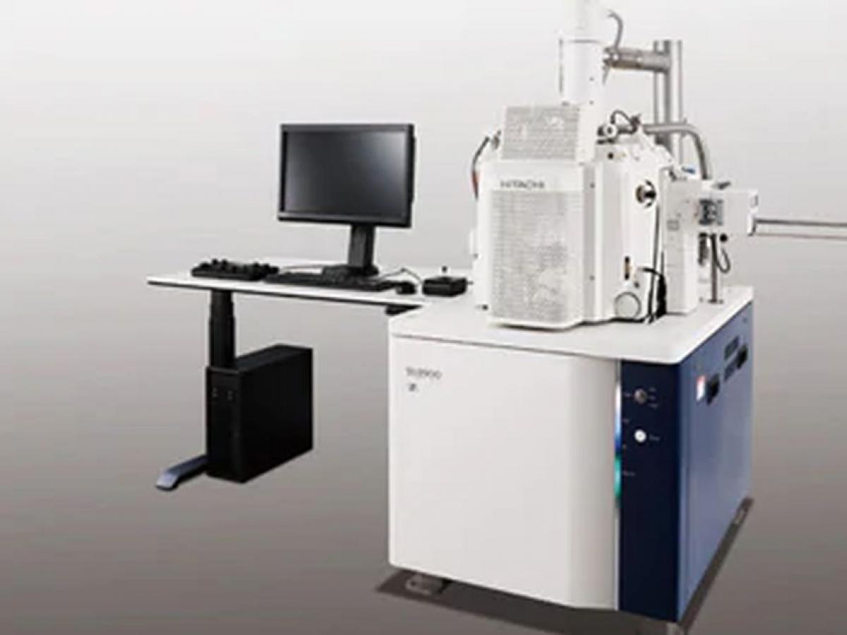
Hitachi SU8600 UHR-SEM
Please contact Mr Ken Neubauer for further information.
Located at Frome Road.
-
Information on the Hitachi SU8600 UHR-SEM
The Hitachi SU8600 is a cold field emission ultra-high resolution scanning electron microscope with secondary electron image resolution of 0.6 nm@15 kV. It equipped with Upper Detector (UD), Lower Detector (LD), Top Detector (TD) and Semiconductor Type BSED (PD-BSED). It has an airlock for fast and smooth sample loading.

Hitachi SU7000 UHR-SEM
Please contact Mr Ken Neubauer for further information.
Located at Frome Road.
-
Information on the Hitachi SU7000 UHR-SEM
The Hitachi SU7000 is an Ultra-High-Resolution Scanning Electron Microscope with Schottky emitter. The large analysis chamber can accommodate large specimen of 200 mm in diameter and of 2 kg. It has UD (Upper Detector), MD (Middle Detector), LD (Lower Detector), PD-BSED (Semiconductor type) and UVD (Ultra Variable Pressure Detector) operating in high vacuum or variable pressure (5 – 300 Pa). It equipped with energy dispersive X-ray spectroscopy (Oxford Instruments Ultim Max 170 and Bruker AXS XFlash 7), electron backscattered diffraction (Oxford Instruments Symmetry S3) and cathodoluminescence detector (Delmic SPARC Spectral). It is capable of high-resolution automated mineralogy (Advanced Mineral Identification and Characterization Software).

Hitachi SU9000 UHR-SEM
Please contact Mr Ken Neubauer for further information.
Located at Frome Road.
-
Information on the Hitachi SU9000 UHR-SEM
The Hitachi SU9000 is a cold field emission ultra-high resolution scanning electron microscope with superior beam brightness and stability. The SE resolution is 0.4 nm @ 30 kV, 1.2 nm @ 1 kV without beam deceleration and 0.8nm with beam deceleration. It can provide images using SE, LA-BSE, HA-BSE and STEM. It equips an energy dispersive X-ray spectroscopy (Oxford Instruments Ultim® Max 100) for elemental analysis.

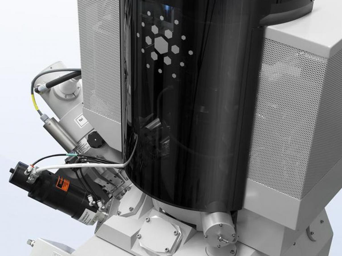
FEI DualBeam™ Focused Ion Beam Scanning Electron Microscope
FEI Helios Nanolab
This instrument is operated by Dualbeam Engineer Dr Animesh Basak.
Located at Frome Road.
-
Information on the FEI Helios Nanolab
Funded by NCRIS, the Helios Dualbeam was installed in Feb 2008.
In a single instrument platform, it combines a high-resolution scanning electron microscope (SEM) with high resolution focused ion beam (FIB).
The FIB uses a focused beam of Ga+ ions to sputter the surface of the sample to expose sub-surface features. The ion beam can also be used to form high resolution images if the beam current is kept low enough to avoid excessive surface sputtering.
The addition of a high-resolution SEM allows the collection of electron-induced signals from the exposed surfaces. These include secondary and back-scattered electron images, characteristic x-ray and electron back-scattered diffraction images for analysis of crystal structure,
crystallographic orientation and phase type. The instrument also has a solid-state STEM detector allowing the imaging of very thin samples.
Instrument capabilities:
- Sample machining
- Sample cross-sections
- 3D microscopy
- Slice and view
- TEM foil preparation
- Atom probe needles
- Feature size measurement
- Site specific sample selection
- Sample selection, placement and shaping
- Micro-analytical investigating
- EDXS - Energy Dispersive X-ray Spectroscopy
- The collection of the emitted x-rays by a solid-state detector and the measurement and display of their energy distribution. This makes possible the identification, quantification and mapping of elements in a solid sample.
- EBSD- Electron Back - Scattered Diffraction
- OIM - Orientation Imaging Microscopy
- The measurements of local orientation by the collection of patterns formed by diffraction of back - scattered electrons within the crystal structure.
- ‘Delpi' - a program which allows the simultaneous collection of EBSD and EDXS data. This makes it Possible to use sample chemistry to aid in phase identification when materials have similar diffraction patterns.
For more details regarding the FIB's capabilities go to:
http://www.feicompany.com/products/families/helios-nanolab-family.aspx

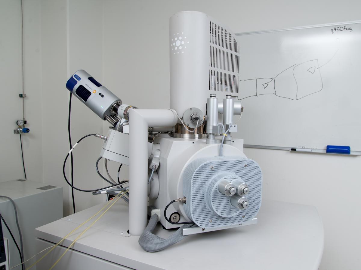
FEI Quanta 450 FEG Environmental Scanning Electron Microscope (ESEM)
Please contact Mr Ken Neubauer for further information.
Located at Frome Road.
-
Information on the SEM FEI Quanta 450 FEG Environmental SEM + Oxford Ultim Max Large Area SDD EDS Detector
The FEI Quanta 450 is a High Resolution Field Emission Scanning Electron Microscope capable of operation in three different modes: High Vacuum, Low Vacuum and Environmental SEM (ESEM). As well as a standard sample stage, the instrument also has cooling, heating and tensile stages. The Quanta 450 is used to image and analyse surface topography and morphology, collect backscattered electron images and characterise and determine a sample's elemental composition via energy dispersive x-ray spectroscopy (EDS). It has an Oxford Ultim Max Large Area SDD EDS detector with Oxford AZtec EDS processing software and also has live mapping functionality.
- High Vacuum mode allows for high resolution imaging of surface topography (up to 1000000x magnification).
- Low Vacuum mode allows for imaging and characterisation of non-conductive samples.
- ESEM mode allows in situ imaging of wet samples, which is ideal for plant material and other biological specimens. It can also be used for in situ observation of processes such as hydration and dehydration, corrosion and crystallisation.
- X-ray analysis for determination of elemental composition with an Oxford Ultim Max Large Area SDD EDS detector with Oxford AZtec EDS processing software.
The stage has a lateral movement range of 100mm and a vertical movement range of 60mm.
Applications for the Quanta 450 are wide ranging and include imaging and microanalysis of metals, semiconductors, materials and their defects, coatings, particles, fibres and geological and biological samples.

Hitachi FlexSEM 1000 SEM
Please contact Dr Gwen Mayo for further information.
Located at Waite facility.
-
Information on the Hitachi FlexSEM 1000 SEM
The Hitachi Flex Scanning Electron Microscope FlexSEM 1000 IIM 1000 features a SE detector, high-sensitivity 4-segment BSE detector and UVB detector, and a pre-centred tungsten filament and accelerating voltages of 1-20 kV.
The ultra-variable-pressure detector enables observation of the surface of non-conducting specimens without coating.

Hitachi SU1510 SEM
Please contact Dr Ben Wade for further information.
Located at Frome Road.
-
Information on the Hitachi SU1510 SEM
The Hitachi SU1510 SEM is a tungsten filament SEM equipped with a secondary electron (SE) detector and a backscatter electron (BSE) detector.
The system allows for variable pressure operation which means non-conductive samples can be imaged uncoated.
With a sample stage that can accommodate samples up to 153mm in diameter the SU1510 is ideal as a pre-screening tool for high resolution SEM samples.

Hitachi SU3800 Automated Mineralogy SEM
Please contact Dr Nobuyuki Kawashima for further information.
Located at Frome Road.
-
Information on the Hitachi SU3800 Automated Mineralogy SEM
Hitachi SU3800 Automated Mineralogy SEM is a tungsten filament SEM equipped with a secondary electron (SE) detector, a backscatter electron (BSE) detector and a cathodoluminescence (CL) detector. The system has a couple of energy dispersive X-ray spectroscopy (Bruker XFlash 6|60) and Advanced Mineral Identification and Characterization System (AMICS) for automated mineralogy. The system is able to accommodate thin sections and round resin blocks (25mm and 30mm).
